In the first part we had the installation of Thonny, the establishment of the Raspberry Pi Pico as well as first application programs for using the inputs and outputs. In the second part It dealt with the programming of the well -known interfaces OneWire, Uart and I2C, all of them second assignments of the pins. Of course, there is still no application for the latest and fastest interface: SPI or Serial Peripheral Interface AKA 4-Wire Bus.
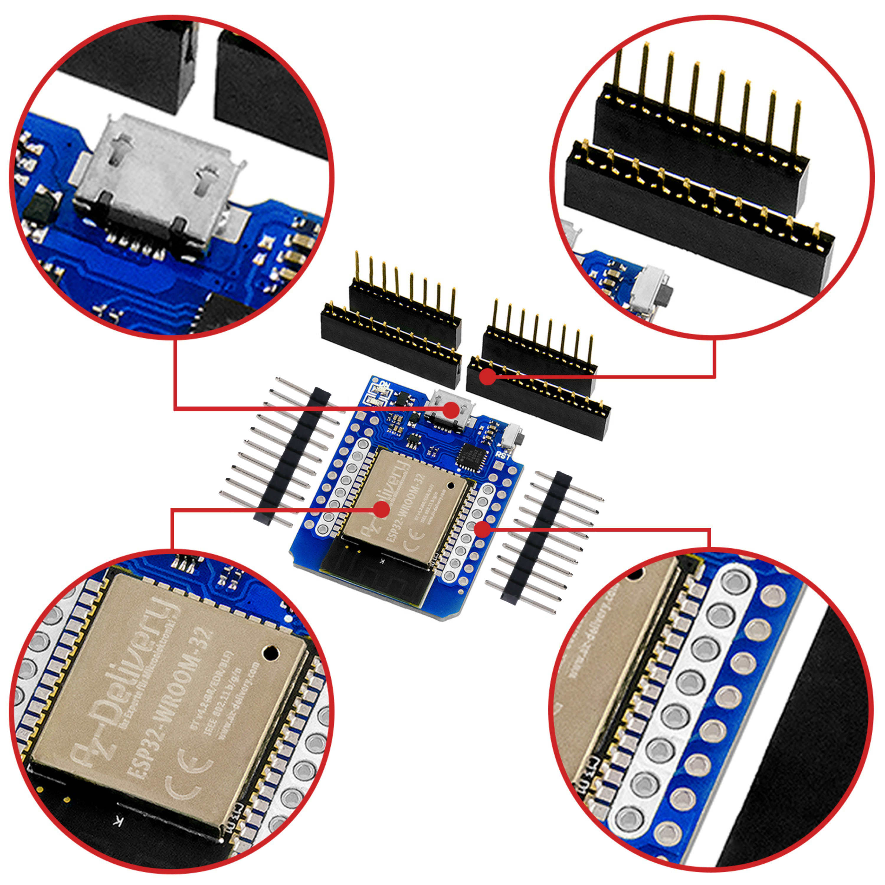
Used hardware
|
1 |
|
|
1 |
|
|
or 2 |
|
|
1 |
MCP23S17 Port Expander alternative click |
|
Div. |
LEDs or rgbled, jumper cable |
I found almost no application for the SPI interface on the Raspberry Pi Pico on the Internet. And if so, then only for simple sensors with C ++, not with micropython. I would like to change that and choose a very useful but also complex IC, the Port Expander MCP23S17, the identical twin of the I2C variant MCP23017.
I have no concrete application in mind, but you can always use 16 additional inputs or outputs, most recently for mine Model railway project with many relay modules. So this time a lot of theory, both for the Raspberry Pi Pico and Spi and McP23x017. Why now the X in the name. As I said, MCP23017 (I2C) and MCP23S17 (SPI) have everything else in common except for the interface to the MCU.
As a reminder: the mostly the same pin assignment of the "twins"

As I said, the difference is the interface that can be found on pins 11 to 14. To the left of the I2C variant (AKA 2-Wire Bus) only SDA and SCK, on the right the four connections for SPI. The naming for the connections is sometimes confusing and, above all, not uniform. And in times of political correctness, two of the possible terms are to be abolished: master and slave. Why is? The "4-Wire Bus" is not only clocked faster, its speed is also due to two data lines. A direction from the controller (former Master) to the peripheral (previously slave), one line goes in the opposite direction.
In the picture the old terms Mosi (master out, slave in) or only si, on some peripheral devices also DI, as well as miso (master in, slave out) or so, also do or sdo. The name for the SPI stroke management is largely standardized, namely SCK. Instead of an address as with I2C, SPI uses a fourth line to initiate data exchange. This also contributes to increasing speed. This connection bears the name SS or CS (Chip Select). The cross -line via CS stands for the negation, i.e. the data transmission takes place if the connection is set to low.
How do you have to imagine this data transmission? The MCP23x17 has storage points, so -called registers in which the microcontroller read data or in which it can write data. Each of these registers has an address, a hexadecimal number with a cryptic name.
In my Micropython program, I listed all the registers with the usual address, even if we will not use everyone.
Register
Iodira = 0x00 # Controls the Direction of the Data I/O for Port A.
Iodirb = 0x01 # Controls the Direction of the Data I/O for Port B.
IPola = 0x02 # configures the polarity on the corresponding gpio-port bits for port A.
IPolb = 0x03 # configures the polarity on the corresponding gpio-port bits for port B.
Gpintena = 0x04 # Controls the interrupt-on-change for each pin of port A.
Gpintenb = 0x05 # Controls the interrupt-on-change for each pin of port B.
DEFVALA = 0x06 # Controls the default comparison value for interrupt-on-change for port A.
DEFVALB = 0x07 # Controls the default comparison value for interrupt-on-change for port B.
INTCONA = 0x08 # Controls how the associated pin value is compared for the interrupt-on-change for port A.
INTCONB = 0x09 # Controls how the associated pin value is compared for the interrupt-on-change for port B.
IOCON = 0x0A # Controls the device.
GPPUA = 0x0C # Controls the pull-up resistors for the port A pins.
GPPUB = 0x0D # Controls the pull-up resistors for the port B pins.
INTFA = 0x0E # Reflects the interrupt condition on the port A pins.
INTFB = 0x0F # Reflects the interrupt condition on the port B pins.
INTCAPA = 0x10 # Captures the port A value at the time the interrupt occurred.
INTCAPB = 0x11 # Captures the port B value at the time the interrupt occurred.
GPIOA = 0x12 # Reflects the value on the port A.
GPIOB = 0x13 # Reflects the value on the port B.
OLATA = 0x14 # Provides access to the port A output latches.
OLATB = 0x15 # Provides access to the port B output latches.
At a second glance you can see a certain systematics in the register names. All names occur quasi twice, with a different last letter A or B. This means the two ports, which represent the actual input or output pins with their eight bits. More about this later.
The IOCON register falls outside this system. We will deal with that later. All registers that have to do with the interrupt function, we will not address in this blog.
As a small change from the gray theory, we now connect the MCP23S17 to the Raspi Pico.
On the following picture the secondary assignments of GP19 = SPI0 TX, GP18 = SPI0 SCK, GP17 = SPI0 CSn as well as GP16 = SPI0 RX are shown on the bottom right. Behind the SPI there is a 0 (zero) in each case, because further SPI interfaces are available. Again two new names: TX for MOSI, RX for MISO. Confusion with UART impossible, because SPI is prefixed. So:
|
Raspberry Pi Pico |
MCP23S17 |
|
GP19 = SPI0 TX (Pin 25) |
SI = Pin 13 |
|
GP18 = SPI0 SCK (Pin24) |
SCK = Pin 12 |
|
GP17 = SPI0 CSn (Pin22) |
Negat CS = Pin 11 |
|
GP16 = SPI0 RX (Pin21) |
SO = Pin 14 |
The port expander requires additional connections:
|
Raspberry Pi Pico |
MCP23S17 |
|
3V3 (OUT) = Pin 36 |
VDD = Pin 9 |
|
GND = Pin 38, 33, 28, 23, 18, 13, 8 oder 3 |
VSS = Pin 10 |
|
HIGH (3V3) oder LOW (GND) |
A0 = Pin 15 |
|
HIGH (3V3) oder LOW (GND) |
A1 = Pin 16 |
|
HIGH (3V3) oder LOW (GND) |
A2 = Pin 17 |
|
3V3 |
Negat RESET über 10 kOhm Pullup-Widerstand |
As I said, I will not use the interrupt pins and functionality. And GPA0 to GPA7 and GPB0 to GPB7 are the gained GPIO connections to which we will connect LEDs or pushbuttons (buttons) on a trial basis.

Back to the program. MicroPython (uPy) provides the hardware support for the microcontrollers via the program module machine. In this the class SPI is declared. So our program starts with loading the modules.
 import machine
 import utime
The instantiation is done with the lines.
 # Assign chip select (CS) pin (and start it high)
 cs = machine.Pin(17, machine.Pin.OUT)

 # Initialize SPI
 spi = machine.SPI(0,
                   baudrate=1000000,
                   polarity=1,
                   phase=1,
                   bits=8,
                   firstbit=machine.SPI.MSB,
                   sck=machine.Pin(18),
                   mosi=machine.Pin(19),
                   miso=machine.Pin(16))
For reading and writing the registers I have inserted short functions which first collect the necessary sequence of device ID, register and if necessary the byte to be written in a buffer, then set CS to LOW, write and if necessary read, and then set CS again to HIGH.
 def reg_write(reg, data):
 # Write 1 byte to the specified device and register.

 # Construct Message (Set ~ W bit low, mb bit low)
     MSG = bytearar()
     MSG.append(Devid)    # Devid Device Opcode
     MSG.append(reg)
     MSG.append(data)
     CS.value(0)
     spi.write(MSG)
     CS.value(1)

 def reg_read(reg, NB=1):
 # Read 1 byte from Specified Register.

 # Construct message
     MSG = bytearar()
     MSG.append(Devid | 1)    # Devid Device Opcode | write bit
     MSG.append(reg)

 # Send Out Spi Message and Read
     CS.value(0)
     spi.write(MSG)
     data = spi.read(NB)
     CS.value(1)
     return data
With the functions reg_write () and Reg_read () as arguments are the name of the register with the variable reg and possibly the byte to be written as a variable data hand over. I had already defined the device name, the Device ID, as Devid = 0x40 at the beginning. This information comes from the data sheet, Figure 3-7, which requires a small slot at this point.

In the reg_write () function, three values are initially saved in the buffer.
- Devid = 0B0100XXXW with X as a placeholder for 0 or 1 depending on a possible device address and W = 0 for writing.
- Reg with the initial -defined register addresses in the Hexadecimal system
- and the data to be written
Only the first two bytes are transferred in the reg_read () function. In order to indicate that the device should send something, the read/write bit must be set to 1 at the end of Devid. Hence the Oder linkage at
MSG.append(Devid | 1) # Devid Device Opcode | write bit
The topic of device addresses will be deepened again with the Iocon tab.
Now we come (finally 😉) to the most important registers, always from above:
Iodir stipulates whether the respective connection should act as an input (= 1) or as an output (= 0). Since I would like to show both without too much effort, I place port A completely as an input (i.e. 0B1111111 = 0xff = 255) and port B completely as exit (i.e. 0b00000000 = 0).
Ipol defines the polarity. As is usually the case today, I will switch the button/buttons against ground, so switch low. Nevertheless, I would like to see the corresponding value as high. For this I need iPola with the value assignment 0b11111111).
We leave out interrupt. Next is
GPPU: For the entrances, it is determined whether the internal pullup resistor should be switched. Since I would like to switch the buttons against GND, I also write 0B11111111 to Gppua.
In order to read the actual value of the GPIOs, I need GPIOA, but the outputs on port B are described via so-called Latch Register (here: Olatb).
All of these stipulations are carried out in the main program, but before the endless loop. There is also a value assignment to the IOCON tab, which I had already mentioned above. This register is responsible for both ports and sets a kind of configuration with every bit. We saw this above in Figure 3-7 of the data sheet.
Here is the information from the data sheet:

With the power-on reset (POR) or reset, all bits are set to 0 (zero). Again we ignore the information on Interrupts. This means that bit 7, bit 5 and bit 3.
Bit 7 defines the nomenclature for the register addresses. The values specified above come from bank 0, which is preset and widespread. The Arduino library also uses this information. So this bit must remain set to 0 (zero).
We only want to describe or read a byte. Therefore, BIT 5 should be set to 1.
And if we want to use several MCP23S17 in parallel and therefore want to determine hardware addresses with the help of the connections A0, A1 and A2, Bit 3 = Haen = Hardware Address Enable Bit must also be set to 1.
So we write in the IOCON register:
reg_write(Iocon, 0B00101000)
Now to the device addresses that cost me a lot of sweat because I first assumed that I can use the same system as for the I2C variant. With the three connections A0 to A2 we have 2 high 3 = 8 different options. At I2C from 0x20 to 0x27.
But while at I2C the highest bit (Bit 7) for reading and writing is set to 0 or 1, it is the lowest bit 0 at SPI. This makes the value of the address bits over a factor of 2 higher. The device address (Device Opcode or Devid) is therefore 0B0100-A2-A1-A0-R/W.
If we do not use the addressing and the R/W-Bit is set to 0 for writing, we receive the basic address 0B01000000 = 0x40. For the connection options from A0 to A2, we must add the following values accordingly. H for high, connection to 3.3V and L for low, i.e. connection to GND.
LLL -> 0x00, i.e. 0x40 (the basic address. LLH -> 0x02, i.e. 0x42. LHL -> 0x04, i.e. 0x44.
LHH -> 0x06, i.e. 0x46. Hll -> 0x08, i.e. 0x48. HLH -> 0x0a, i.e. 0x4a. HHL -> 0x0c, i.e. 0x4c. And finally HHH -> 0x0e, i.e. 0x4e.
Anyone who knows the I2C variant with the I2C addresses 0x20 to 0x 27 will see at a glance that the address at Spi is exactly twice as large. And the double of 0x25 is Not 0x50, but 0x4a. After all, we count in the Hexadecimal system.
Enough the gray theory and above all mathematics, now it should flash.
On the connections GPB0 to GPB2 I connect a RGbled that changes the color in my endless loop in the quick change, while in the Python Shell (Repl = Read-EvalUate-Print-Loop) it is displayed, which input on port A I with help a jumper cable on gnd lay.
Here mine Sample program for download. You can easily adjust it for your purposes.
This explains the basics for the Port Expander with a SPI interface on the Raspi Pico and you can exploit the diverse possibilities of the GPIO pins gained. If you want to know more about Spi: here I found a good introduction.
Here the circuit diagram and the pint table for the basic circuit:

|
MCP23S17 |
Raspberry Pi Pico |
|
Si = pin 13 |
GP19 = SPI0 TX (PIN 25) |
|
Sck = pin 12 |
GP18 = Spi0 Sck (Pin24) |
|
Negat CS = PIN 11 |
GP17 = SPI0 CSN (PIN22) |
|
So = pin 14 |
GP16 = SPI0 RX (PIN21) |
|
VDD = PIN 9 |
3V3 (out) = pin 36 |
|
VSS = PIN 10 |
GND = PIN 38, 33, 28, 23, 18, 13, 8 or 3 |
|
A0 = pin 15 |
High (3V3) or low (GND) |
|
A1 = pin 16 |
High (3V3) or low (GND) |
|
A2 = PIN 17 |
High (3V3) or low (GND) |
|
Negat reset over 10 kohm pullup resistance |
3V3 |


1 commentaire
junzo yoshida
pico spi michropython
thamk you wonderful page